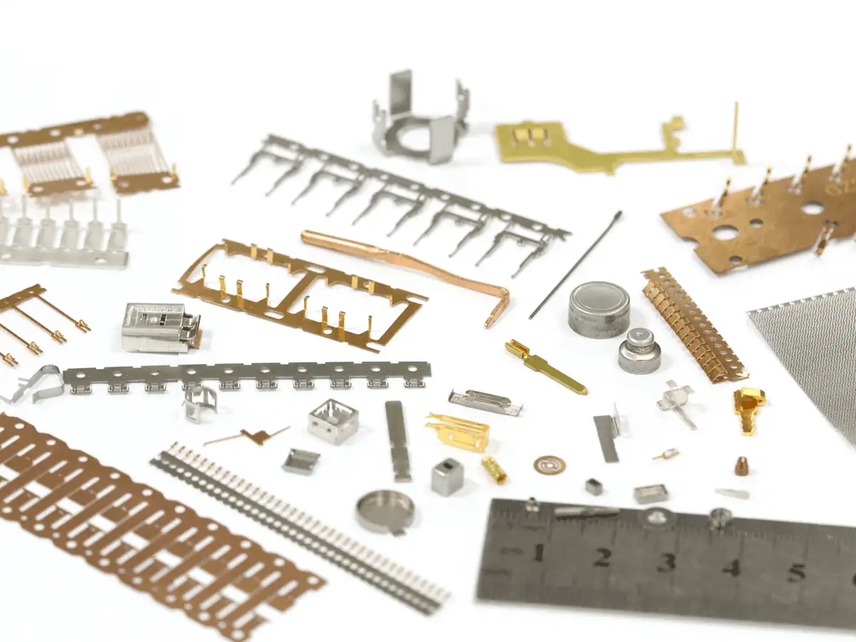
Stamped Parts / Lead Frames

Stamped Lead Frames

A lead frame is a thin metal plate to which semiconductors are attached during the device assembly process. Also called a leadframe, this thin-layered, metal component connects the wiring from tiny electrical terminals on the semiconductor surface to the large-scale circuitry on automotive applications, electrical devices and circuit boards. Quality of lead frames is vital, as any tiny defect can adversely impact semiconductor adhesion and ultimately render the greater assembly inoperable.

±0.002mm
Tolerance Control
1,500+ SPM
Stamping Speed
100% Burr-Free
Edge Quality
0.10mm
Min Thickness

Make sure the semiconductors used in your process operate effectively with high-quality lead frames manufactured by Kravzik. We are a precision supplier of stamped metal parts and assemblies for use in a variety of industries. Our specialty is high-precision stamped lead frames for automotive, electronics, electrical and mechanical applications.

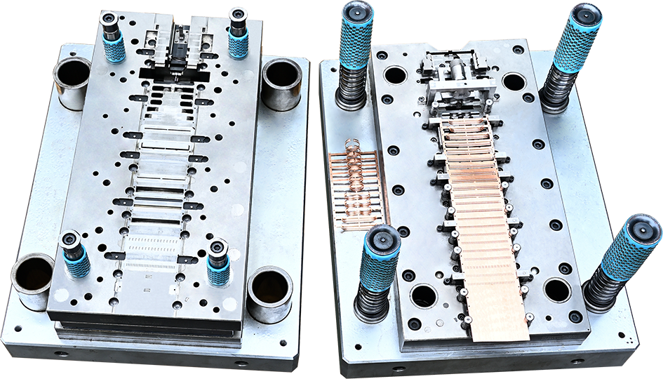
As a dedicated lead frame manufacturer, we produce stamped leadframes for IC packaging deployed across QFN, SOIC, QFP, DIP, BGA, optocoupler, and ASIC packages. Manufactured in an IATF 16949 certified facility with 100% burr-free micro-hole perforation at speeds exceeding 1,500 SPM.

Quality Assurance

At Kravzik, quality is our utmost priority. We conduct a feasibility review on the part to ensure manufacturability at the start of every program. A run-at-rate study is also implemented on the first run to ensure quality before large-scale production. This enables our quality and production management teams to monitor controls closely and make sure jobs run smoothly. Manufacturing continues once testing checks out, and the first batch of conforming parts is manufactured.

Our quality management system is comprised of sophisticated quality technology and controls, continuous improvement programs, and a superior quality laboratory and management team. Throughout our production plant, we deploy in-line/off-line camera vision systems and sensor technology, designed and fabricated unique to every production program. Our vision system technology operates in coordination with our stamping production machinery to thoroughly inspect and identify part features and dimensions with automated camera imaging. This quality control process ensures every part produced with our stamping equipment always yields 100% quality and zero defects.

One size does not always fit all when it comes to the design and manufacture of lead frames. Custom specifications and design features that improve performance are necessary. With extensive experience manufacturing custom lead frames for critical applications, Kravzik is your precision lead frame manufacturing partner.

Specifications

Past Lead Frame Specifications

Representative dimensional capabilities achieved across production lead frame programs. Custom specifications engineered to your requirements.

ParameterMinimumMaximumNotes
Part Length / Width0.25 in (6.35 mm)7 in (177.8 mm)Standard progressive die range
Part Thickness0.002 in (0.051 mm)0.090 in (2.2 mm)Ultra-thin to medium gauge
Part Diameter0.25 in (6.35 mm)7 in (177.8 mm)Round / cylindrical parts
Tolerance± .001 in (± .025 mm)Positional tolerance dependent on feature
Press Speed1,500 strokes/minBruderer-class high-speed presses
Press Rating30 tons200 tonsProgram-dependent
Coplanarity0.05mm across stripLaser profilometry verified
Burr Height10 microns (0.01mm)100% in-die vision inspection

Critical Risks in Lead Frame Stamping

Each risk is identified, quantified, and mitigated through engineered stamping process design — not through post-process inspection alone.

Coplanarity Deviation

Impact: Non-flat leadframes cause die attach failure, wire bonding misalignment, and package warpage during molding. Even sub-micron variance across the strip can render hundreds of IC packages defective.

Solution: Precision-guided stripper plates with micro-adjustable die clearance. In-die coining stations that stress-relieve the strip before final blanking. Continuous laser flatness measurement at 100% inspection rate across the full strip.

Micro-Burr Formation

Impact: Burrs exceeding 10 microns disrupt wire bonding, create unintended short circuits, and contaminate cleanroom assembly environments. A single burr can cause cascade failure across the entire production lot.

Solution: Ultra-fine-grain tungsten carbide tooling with polished cutting edges maintained to sub-micron sharpness. Progressive die stations with dedicated burr-suppression geometry at each cutting operation. In-die vision cameras positioned after every forming station.

Edge Deformation & Micro-Cracking

Impact: Stressed edges lead to lead bending during trim/form operations and latent field failures under thermal cycling. Micro-cracks propagate over time, causing intermittent connectivity failures that are nearly impossible to detect in post-production testing.

Solution: Optimized punch-to-die clearance ratios calibrated to each material thickness. Radius-controlled cutting edges with multi-stage shaving stations that progressively refine the sheared surface. Stress-relief annealing integrated into the progressive die sequence.

Design Features

Metal Stamping Design Features

Kravzik offers a comprehensive range of stamping design features to meet your unique requirements across every lead frame program.

Bi-Metal
Coated
Coined
Compliant Pin
Countersunk Holes
Critical Dimensions
EB Welded
Embossed
Enameled
Eyelets
Flat
Formed
Heat-Treated
IDC Slots
Injection Molded
Inlay
Insert Molded
Multiple Stamping
Numbering
Powder Coated
Precious Metal Plated
Reeled
Riveted
Shape Critical
Skived
Stacked
Strain Relief
Surface Critical
Surface Mounted
Tapped
Threaded
Tip Coin
Tox Lock
Tuning Forks
Welded

Post-Operations

Post-Stamping Operations

To complete finished production parts, we offer final post-production process operations prior to product packaging and delivery.

Heat Treatment

Stress relief, annealing, and hardening to meet mechanical property specifications.

Deburring

Vibratory, thermal, and mechanical deburring for 100% burr-free edges.

Washing / Degreasing

Multi-stage aqueous cleaning systems for contamination-free parts.

Post-Plating

Finish plating after forming. Pre-plating option also available.

Hardware Installation

In-die hardware assembly and post-production hardware insertion.

Materials

Metal Stamping Materials

Although each metal has its own blend of mechanical, chemical and surface properties, our knowledgeable engineering and production teams have decades of experience and can achieve optimum results from a variety of metals. Our team develops the right tooling techniques to ensure the unique properties of any metal yield exactly what our customers require.

MaterialComposition% IACSTensile StrengthPrimary Applications
C19400 (Cu-Fe-P)Copper-Iron-Phosphorus65450–550 MPaGeneral-purpose IC leadframes, consumer electronics
C70250 (Cu-Ni-Si-Mg)Copper-Nickel-Silicon-Magnesium43650–750 MPaHigh-strength power modules, automotive EV
Alloy 42 (Fe-42Ni)Iron-42% Nickel3550–650 MPaLow-expansion ceramic packages, military/aerospace
C18150 (Cu-Cr-Zr)Copper-Chromium-Zirconium80480–560 MPaHigh-conductivity power semiconductors
C10200 (OFHC Copper)Oxygen-Free High-Conductivity Copper101220–280 MPaUltra-high conductivity, RF/microwave leadframes
CopperPure Copper (C11000)100220–310 MPaStandard conductivity applications
BrassCopper-Zinc (C26000)28350–480 MPaDecorative/corrosion-resistant applications
Stainless Steel304 / 3012-3520–860 MPaHigh-strength, corrosion-resistant environments
Phosphor BronzeCu-Sn-P (C51000)15380–650 MPaSpring contact, fatigue-resistant applications
Beryllium CopperCu-Be (C17200)22690–1,380 MPaHigh-strength, high-fatigue electronic connectors
AluminumAl 1100 / 505235-6090–250 MPaLightweight, thermal management applications
TitaniumTi Grade 23345–480 MPaMedical implant, aerospace, lightweight structural

Plating

Plating Material Finishes

We offer a range of pre- and post-plating options for metal stamping assemblies allowing for corrosion protection, electrical conduction, decorative use, wear resistance, coloring, bonding, and lubricity. Choose between overall plating, select plating, or spot plating application. Stampings can be reel-to-reel plated, barrel plated, rack plated, vibratory plated, or selective-loose-piece plated.

Copper
Nickel
Tin-Lead
Tin
Palladium
Palladium-Nickel
Silver
Gold
Zinc

Surface Coatings

Surface Coating Applications

Stampings may require a surface coating for dielectric insulation, application environment protection, heat and extreme temperature protection, abrasion protection and corrosion protection in various electrical applications. Coatings can be applied through fluidized bed dip process, electrostatic fluidized bed dip process and electrostatic spray process.

Epoxy Powder Coating
Nylon Powder Coating
PVC Powder Coating
Polyethylene Powder Coating
Polyurethane Powder Coating
Polyester Powder Coating
Vinyl Powder Coating
Vinyl Plastisol Liquid Coating

Assembly

Stamping Assembly Processes

Kravzik offers complete stamping and product assembly with all manufacturing processes under one roof. We provide a cost-effective finished product with particular attention to quality, production deadlines, and the feasibility of end-use.

Automated In-Die Assembly
Automated Robotic Assembly
Secondary Semi-Automated Assembly
Threading
Staking
Tapping
Hardware Insertion
Joining
Stacking
Welding
Riveting

Hardware

Assembly Hardware & Part Installations

For assembled applications, parts may require joining of metal hardware, plastic parts or metal inserts. Hardware installation can be performed in-die during the stamping process or as a secondary operation.

Plastic Pieces
Metal Inserts
Fasteners
Screw Machine Parts
Pemserts
Bushings
Nuts
Studs

Lead Frame Applications by Industry

Precision leadframes engineered for every semiconductor packaging requirement.

Semiconductor

QFNSOICQFPDIPBGAOptocouplerASIC leadframes

Automotive EV & E-Mobility

IGBTMOSFETPower moduleECULiDARInverter leadframes

Telecommunications

RF moduleOptical transceiverBase stationRouterAntenna leadframes

Consumer Electronics

SMD LEDDisplay driverCamera sensorWearable device leadframes

Medical & Healthcare

Pacemaker ICBiosensorHearing aidUltrasoundImplantable leadframes

Industrial & Machinery

Motor drivePLC controllerIndustrial relayPower supply leadframes

Frequently Asked Questions

What is a leadframe?+
A leadframe is a thin metal plate that serves as the electrical interconnect between semiconductor die and external circuitry. Manufactured through high-precision stamping or etching, leadframes provide both mechanical support and conductive pathways for IC packages including QFN, SOIC, QFP, DIP, and BGA formats. The quality of the leadframe directly determines semiconductor adhesion, wire bonding integrity, and overall package reliability.
What materials are used for lead frames?+
The most common materials for custom lead frames include copper alloys (C19400 for general-purpose, C70250 for high-strength, C18150 for high-conductivity, C10200 for ultra-high conductivity) and iron-nickel alloys (Alloy 42 for low thermal expansion ceramic packages). Material selection depends on electrical conductivity requirements, thermal dissipation needs, mechanical strength, and the specific semiconductor packaging process.
What tolerance can you achieve on stamped lead frames?+
Our high precision lead frames achieve positional tolerance of ±0.002mm and coplanarity within 0.05mm across the full strip. These tolerances are maintained consistently across production volumes exceeding millions of units per run — verified by in-die vision systems, automated optical inspection (AOI), and laser profilometry at 100% inspection rate.
What is the difference between stamped and etched lead frames?+
Stamped leadframes are produced through progressive die stamping — a high-speed, cost-effective mechanical process suitable for high-volume production (1,500+ SPM). Etched leadframes are chemically machined and offer finer feature resolution but at higher unit cost and lower throughput. Stamped leadframes are preferred for most commercial IC packaging; etched is used for ultra-fine pitch or low-volume specialty packages.
Do you support custom leadframe designs?+
Yes. As a specialized lead frame manufacturer, we work directly with your engineering team from initial design review through tool development and full production. Our in-house tooling department develops progressive stamping dies for any custom leadframe geometry. Feasibility analysis and DFM feedback provided within 24 hours of receiving your drawings.
What plating options are available for leadframes?+
We offer a comprehensive range of plating finishes including silver (spot and overall plating), nickel-palladium-gold (Ni/Pd/Au PPF pre-plated leadframes), selective gold plating, tin, and solder plating. Application methods include reel-to-reel, barrel, rack, and vibratory plating. Plating thickness is verified by 100% XRF measurement.
Custom Lead Frame Quote

Submit your drawings and target volumes. DFM analysis and quotation within 24 hours.

Package TypeMaterialTolerancePlatingAction
QFN Lead FrameC19400±0.002mmAg / NiPdAu PPFRFQ →
SOIC Lead FrameC70250±0.002mmAg spot platingRFQ →
QFP Lead FrameAlloy 42±0.003mmSolder plate / PPFRFQ →
Power ModuleC18150±0.002mmAg / Ni flashRFQ →
Custom Lead FrameSpecifyConsultConsultRFQ →